Speakers
Plenary Speakers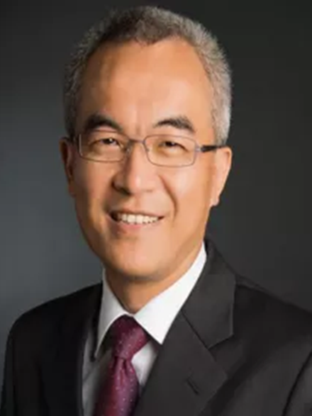 |
"Advance Heterogeneous Integration package solution for Silicon Photonics application" Scott Chen (Advanced Semiconductor Engineering, Inc.) Abstract: Heterogeneous Integration (HI) is the key technology to extend Moore's Law in semiconductor. The advanced packaging integrated solution has been enable high computing performance. Silicon Photonics solution of CPO (Co Package Optics) would be main trend and solution to improve the bandwidth and reduce much power consumption. TSV and FanOut and other advanced package solution (VIPack) would support CPO / Datacenter of Silicon Photonics technology application; PowerSIP by vertical regulator module would lower and manage the power consumption. |
 |
"Silicon Photonic MEMS Switch for AI Super Computers" Ming Wu (University of California, Berkley) Abstract: Programmable optical interconnect offers significant advantages for AI supercomputing clusters. Tens to hundreds of GPUs/TPUs/xPUs connected by optical circuit switches enable reconfiguration of network topology for specific AI workloads. It also increases machine availability, resilience, and physical isolation for multi tenants, in addition to significant reduction in capital and operation expenditures and power consumption. Recently, Google has reported the integration of optical circuit switches in their TPU v4 AI supercomputers and data centers. Previously, high radix optical switches can only be made using free space optics. In this talk, I will introduce silicon photonic MEMS (micro-electro-mechanical systems) technology. By integrating MEMS switching elements with silicon photonics, high-radix switches can be integrated on a single chip. |
 |
"Silicon Photonics Light Engines with 2.5/3D Heterogeneous Integration" Radhakrishnan Nagarajan (Marvell Technology) Abstract: AI data center deployments have pushed the speed of optical interconnects from 800 Gbit/s to 1.6 Tbit/s and beyond, while placing a premium on power, performance and latency. In this talk, we discuss the use of 2.5D/3D heterogeneous integration, where separately manufactured electronic and optical components are assembled on to an active silicon photonics interposer to form a Light Engine, to enable low energy, high density high speed optical interconnects for these applications. |
 |
"Chiplet and Advanced Packaging Research Ecosystem" John Knickerbocker (International Business Machines Corporation) Abstract: Multi-chiplet based architectures offer the opportunity for (1) reduced time to new products using smaller chiplet sizes that also provide higher chip yield and (2) lower system cost from reuse of chiplet functional blocks and use of industry optimized "standard chiplet offerings." Advanced packaging innovations have led to increasing options of materials, structures, equipment and processes. Fine pitch I/O with chiplet to chiplet interconnection with electrical interconnection and photonic links are becoming increasingly important for high performance applications. This presentation will provide examples of increasing ecosystem capabilities and model / hardware demonstrations to support technology advancement. |
IEEE EPS Special Speakers
 |
"Technologies for Chiplet based System Integration" Tanja Braun (Fraunhofer IZM) Abstract: The economic advantages of silicon scaling according to Moore's Law have gone, as today, only a limited number of foundries can afford the manufacturing of high-end nodes. Now, heterogeneous integration in combination with advanced packaging are the path to achieve economic advantages and also to enable new applications. Many options for the package including silicon interposers, Fan-out on substrate, and variations of 3D stacking approaches are seen as possible solutions. However, performance of current applications requires still more transistors per system, but industry also needs a new, more economical system packaging approach. Chiplets are considered the main solution to address this challenge. Besides all the design aspects, packaging of Chiplet-based systems also holds quite some challenges and requires advanced packaging approaches. The presentation will summarize different advanced packaging solutions as Flip Chip on organic, silicon or fan-out interposer and discuss key challenges as e.g. warpage and possible mitigation solutions. |
 |
"Mechanical Behavior of Solder Micro Bumps in Advanced Packaging for Heterogeneous Integration" Jeffrey Suhling (Auburn University) Abstract: Micro bump solder interconnections are typically utilized in advanced packaging architectures employed for heterogenous integration such as System in Package (SIP), 2.3D, 2.5D, 3D, etc. Since the volume of solder in each micro joint is so small, there is typically only one anisotropic single crystal tin grain in each joint that is reinforced with Sn-Ag or Sn-Cu intermetallic particles. In this presentation, the mechanical behavior of micro bumps in advanced packaging will be summarized and its practical use discussed. A set of 6 unique elastic compliances are used to model the elastic behavior of a reinforced body-centered tetragonal tin crystal, while the post yielding responses beyond the elastic limit are predicted using Crystal Plasticity (CP) theory with 10 different slip families and 32 slip systems. Mechanical response simulations have been performed with the crystal plasticity-based DAMASK code as well as with ABAQUS UMAT subroutines. Several results will be presented including: (1) characterization of the elastic compliances of single crystal SAC solders using nanoindentation, (2) calibration of crystal plasticity material constants for single crystal SAC solders using uniaxial and shear testing, (3) machine learning models to predict the orientation dependent deformation behavior of single crystal SAC micro joints, and (4) simulation of micro joint deformations and strains in area array assemblies. |
Special Speakers
 |
"Innovation and steps in hetero-integration" Harald Kuhn (Fraunhofer ENAS) Abstract: The rapidly evolving landscape of semiconductor technology demands innovative approaches to overcome the challenges of hetero-integration in process technology, test and reliability. This presentation explores key aspects, highlighting three critical areas for a wide range of micro assembly applications: One of the pivotal elements in the fabrication of heterogeneous integrated systems is wafer bonding technology. This section delves into the complexities and advancements of these wafer to wafer bonding techniques, highlighting their critical function in heterogeneous integration using the example of chemical mechanical planarization (CMP). It encompasses an examination of the latest technologies and their impact in semiconductor devices. The integration of digital twins and artificial intelligence within CMP as an example is another key area of focus. This entails an exploration of how AI-driven digital twins enhance process control and optimization in semiconductor manufacturing, resulting in more precise control and increased efficiency in CMP processes. Ensuring the quality and reliability of heterogeneous integrated systems remains paramount concern. This segment addresses the distinct challenges and established procedures for testing and ensuring the long-term reliability of these advanced semiconductor devices. It will discuss the methods for verifying functionality and durability in these complex systems. By examining these key areas, this presentation provides valuable insights into the intricacies and solutions with hetero-integration, driving innovation, research and future advancements for use with the next generation semiconductor test applications. The increasing complexity requires new solutions for testing, e.g., DfT, KGD up to advanced test systems. |
 |
"Wireless Power Transfer Theory Established Last Decade" Takashi Ohira (Toyohashi University of Technology) Abstract: Wireless system applications of CPMT started in the 20th century mainly intended for RF broadcasting and telecommunications. While those two schemes are getting well matured and sophisticated now, the third potential has strongly emerged in this century, i.e., wireless power transfer (WPT). This special talk lectures on what exactly is needed for WPT system design and the crucial (but basic) theories developed last decade. |
 |
"Wafer-scale packaging of photonic switches and transceivers" Geert Van Steenberge (imec and Ghent University) Abstract: Today, despite the use of complex photonic integrated circuits (PICs), the fabrication of a complete optical device still requires a large amount of sequential assembly steps. Integration of PICs, electronic interface circuits, III-V optical gain elements and fiber attachment parts is still based on manual processes on the level of individual devices, limiting scalability and cost efficiency. To reduce the packaging cost and reach the full potential of integrated photonics, a more disruptive approach is required, shifting complexity from sequential assembly on device level to parallelized planar fabrication on substrate- or wafer-level. Within the Horizon Europe project PUNCH, semiconductor packaging technology compatible with high-volume manufacturing is leveraged for providing full thermal, electrical, and optical packaging solutions. The development of a III-V foundry process for micro-transfer-printing compatible semiconductor optical amplifiers enables lossless optical switching on a silicon photonics platform. Custom designed electronic ICs to actuate, control, and power-monitor scaled switch fabrics are densely integrated with the photonic ICs into a heterogeneous fanout wafer-level package (FOWLP), processed on a 200 mm reconstructed wafer platform. In addition, the optical interfacing to the photonic ICs is accomplished using an optical redistribution layer, providing an optical fanout on organic IC-substrates, and allowing for a scalable optical fiber packaging solution. While PUNCH revolves around photonic switches and transceivers, the packaging solutions are generic and have a wide application potential. |
Invited Speakers
| Hybrid Bonding: | |
|---|---|
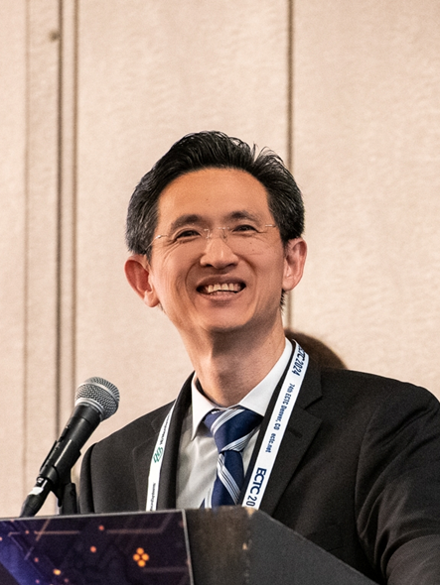 |
"Hybrid Bonding in Advanced Heterogenous Integration: Key Metrology Enablers" Bongsub Lee (Adeia Inc.) |
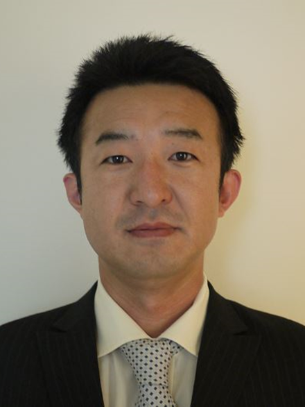 |
"CMOS Directly Bonded to Array (CBA) Technology for Future 3D Flash Memory" Masayoshi Tagami (KIOXIA Corporation) |
 |
"Next-Generation Wafer-to-Wafer Bonding Technologies for Sub-50nm Bonding Overlay Accuracy" Tomohiro Chiba (Nikon Corporation) |
 |
"Fine pitch die-to-wafer hybrid bonding integration" Ye Lin (imec) |
| ---------------------------------------------------------------------------------------------------- | |
| Adv. Packaging and Emerging Technologies: | |
 |
"In-line SEM Evaluation Technique for Cu Pad Nanotopography for Hybrid Bonding Applications" Hiroaki Kasai (Hitachi High-Tech Corporation) |
| ---------------------------------------------------------------------------------------------------- | |
| Process and Material Technologies: | |
 |
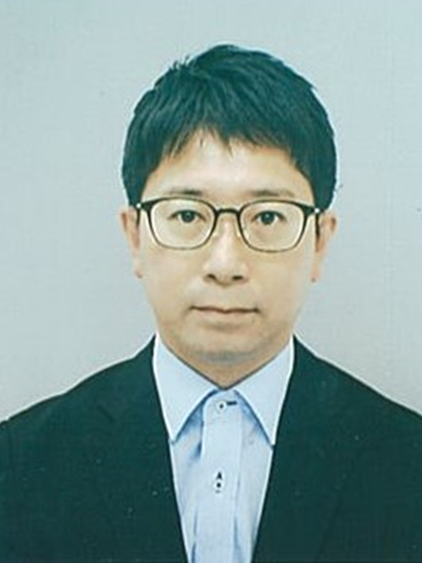
"Polymer Optical Waveguide for Silicon Photonics" Nobuyuki Otozawa (AGC Inc.) |
 |
"Thermally Stable Solder Resist for High Temperature Applications" Daisuke Shibata (Taiyo Ink Mfg. Co., Ltd.) |
| ---------------------------------------------------------------------------------------------------- | |
| Bioelectronics and Healthcare: | |
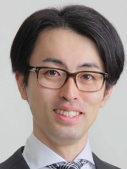 |
"Wearable Electronic Packaging Technology for VR and Biomedical Applications" Seiichi Takamatsu (Thomas J State University of New York at Binghamton) |
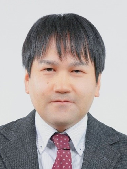 |
"Wood Nanocellulose-Based Green Electronics" Hirotaka Koga (Osaka University) |
| ---------------------------------------------------------------------------------------------------- | |
| Power Electronics: | |
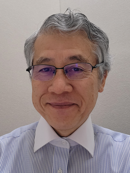 |
"Recent progress and task of GaN materials and devices for power applications" Yohei Otoki (Nagoya University, National Yang Ming Chiao Tung University) |
| ---------------------------------------------------------------------------------------------------- | |
| Automotive and EMC: | |
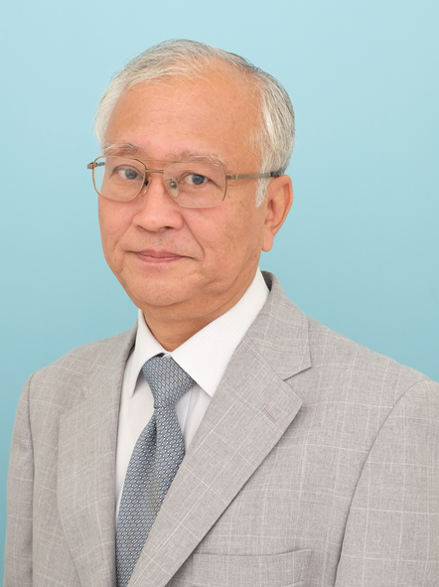 |
"EMC overview, Causes and Physics" Hideho Yamamura (Ultimate Technologies Inc.) |
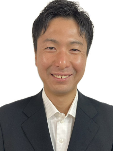 |
"Application of EMC Simulation Including Semiconductor for Short-term Development" Kazuki Furukawa (AISIN CORPORATION) |
| ---------------------------------------------------------------------------------------------------- | |
| IEEE EPS Technical session: | |
 |
"Advanced Materials and Processes for Glass-core Packaging" Mohan Kathaperumal (Georgia Institute of Technology) |
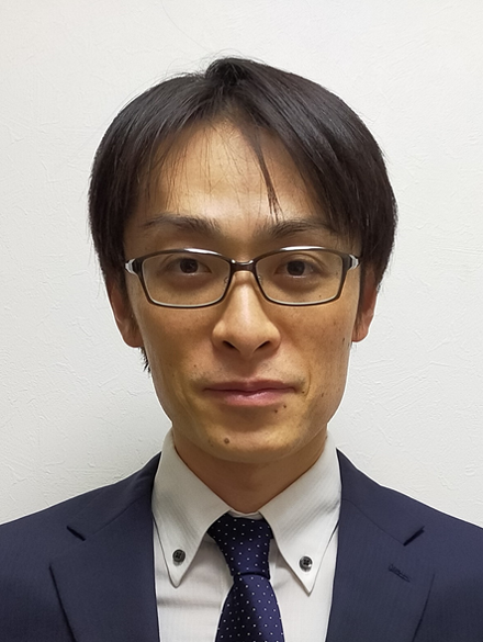 |
"Glass materials and glass structuring technologies for glass-core substrates" Yoichiro Sato (AGC Inc.) |
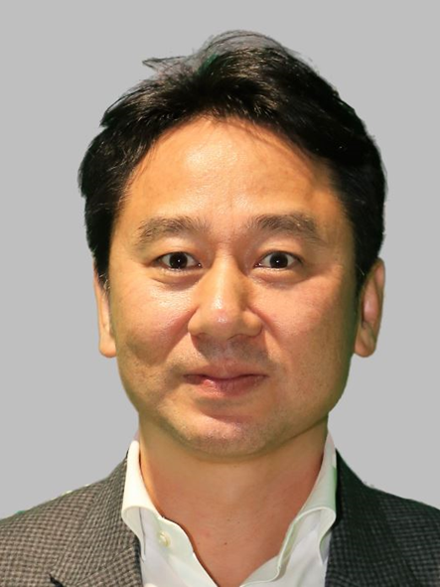 |
"Reliability Assessment of Glass Substrate/Interposer" SB Park (Binghamton University) |
