Speakers
Plenary Speakers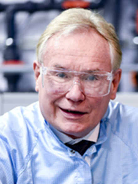 |
""Nothing" is Better than Silica" Sir David Neil Payne (University of Southampton) Abstract: Conventional optical fibres guide light through transparent solid glass cores. Since their invention in in the 1960s, they have become the backbone of global communications with around 500 million km installed every year. 45 years later, we have a new low-loss hollow core fibre (HCF). We are now able to the use air as the transmission medium with guidance provided by a carefully structured metamaterial in the fibre cladding. This provides all the advantages of solid fibres, but without the limitations associated with the core glass. We can have 30% lower latency, >1000 times lower nonlinearity and the potential for propagation loss of only 0.03 dB/km, low enough for repeaterless transoceanic distances. When commercially cabled (packaged) and produced in large volumes, this will enable a significant increase in the transmitted data transmission capacity and reduction in the cost-per-bit, which will revolutionise global optical communications once again. With the huge increase in data traffic comes a headache in how to store the information for the requisite period of time that is often mandated by banks and government – up to several hundred years. Once again, silica comes to the rescue and a new storage medium based on silica disks appears a leading contender to replace today's tape units. The technique, known as 5D storage because of the way each bit can be written and read, provides both high storage density and an extraordinary lifetime estimated at thousands of years. |
 |
"Paradigm Shifts in Silicon Photonics" Roel Baets (Ghent University - imec) Abstract: Silicon photonics has become a mature enabling technology for high speed transceivers in data centers and related applications. Evolutions in the data center area, in particular those driven by the rapidly growing demand for more powerful and more energy efficient AI solutions, as well as a broad set of entirely different emerging applications, imply that the established silicon photonics technology solutions need to be adapted so as to enable higher performance, new applications and new spectral bands. This is now leading to a wide variety of new approaches in silicon photonics, especially with respect to heterogeneous integration of new materials. |
 |
"Challenges and Opportunities for Japan Ecosystem in CoWoS® Technology Development for Further Evolution of AI" Shimpei Yamaguchi (TSMC Japan 3DIC R&D Center, Inc.) Abstract: Recent significant booming in high performance computing (HPC), represented by generative AI, is leading semiconductor market growth. The trend is enabled by evolution of advanced packaging technology such as tsmc CoWoS®. TSMC Japan 3DIC R&D Center was established in 2021 to drive future process and material pathfinding for advanced packaging together with ecosystem partners in Japan. In this talk, we will describe the key challenges in CoWoS packaging and the latest progress of the collaborative research focusing on packaging materials, process, and substrates. Outlook and direction of the technologies will be also discussed. |
IEEE EPS Special Speakers
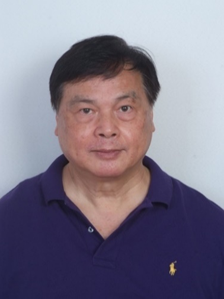 |
"Co-Packaged Optics – 3D Heterogeneous Integration of Photonic IC and Electronic IC" John H Lau (Unimicron Technology Corporation) Abstract: Co-packaged optics (CPO) are heterogeneous integration packaging methods to integrate the optical engine (OE) which consists of photonic ICs (PIC) and the electrical engine (EE) which consists of the electronic ICs (EIC) as well as the switch ASIC (application specific IC). The advantages of CPO are: (a) to reduce the length of the electrical interface between the OE/EE (or PIC/EIC) and the ASIC, (b) to reduce the energy required to drive the signal, and (c) to cut the latency which leads to better electrical performance. In the next few years, we will see more implementations of a higher level of heterogeneous integration of PIC and EIC, whether it is for performance, form factor, power consumption or cost. |
 |
"Aging of Lead-Free Solders" Jeffrey C. Suhling (Auburn University) Abstract: In this talk, an overview of our research on the effects of aging on the mechanical behavior of lead-free solders is presented. This work as involved a combination of experimental material characterization and measurements of microstructural evolution, as well as constitutive model development and finite element predictions of reliability. Stress-strain and creep tests have been performed using miniature tensile samples, and the degradations in the effective elastic modulus, yield stress, ultimate tensile strength, and creep strain rate have been characterized and modeled as a function of aging temperature, aging time, and alloy composition. Analogous results have also been obtained using nanoindentation testing of small solder joints from lead free electronic assemblies. Finally, cyclic stress-strain testing has been utilized to understand the aging induced degradations in the hysteresis loop and fatigue life. The results of the experimental mechanical testing have been correlated with observations of microstructural evolution occurring in lead free solders during aging to develop a fundamental understanding of the causes of the material property degradations. In addition, they have been used to build aging effects into the Anand viscoplastic constitutive model as well as a modified Morrow model for fatigue life, and then implemented in finite element simulations to make reliability predictions for electronic products subjected to aging |
Special Speakers
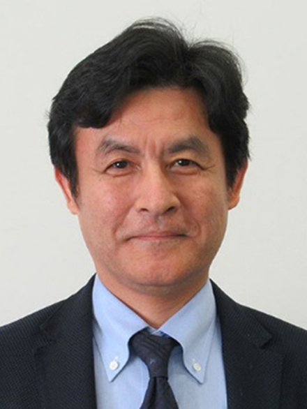 |
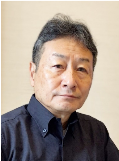
"Artifact Metrics and Individual Management of Semiconductor Packages" Tsutomu Matsumoto (AIST) Abstract: Artifact metrics refer to the measurement of characteristics of individual man-made objects, providing smarter object verification, identification, and authentication capabilities. This paper discusses artifact metric systems, each of which recognizes intrinsic random structures formed on the surface of semiconductor packages and examines the potential of such systems to achieve individual management of semiconductor packages with remarkable accuracy. These intrinsic structures can be manufactured using special inkjet printing or certain nanotechnologies. |
 |
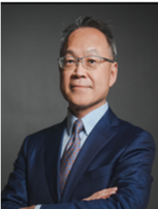
"Advanced Packaging Technologies Enabling AI Semiconductors at Applied Materials" Noriaki Matsunaga (Applied Materials Japan) Abstract: Applied Materials develops advanced packaging technologies that play a key role in enabling next-generation AI semiconductors. This presentation introduces innovations in hybrid bonding, wafer-level integration, and high-density interconnects designed to meet the performance, power, and scaling requirements of AI workloads. Through expertise in materials engineering, process control, and inspection, Applied Materials provides integrated solutions that support heterogeneous integration and system-level optimization. These technologies contribute to faster data processing, reduced latency, and improved energy efficiency in AI chips. Attendees will gain insights into how advanced packaging is helping shape the future of artificial intelligence and high-performance computing. |
 |
"Innovative AI for Advanced Packaging Solutions" C.P. Hung (ASE Group) Abstract: Advanced packages deliver increasing density interconnect between chips and are implemented as enabling technologies for ultrahigh performance module or system. This presentation will explore the AI/ML technologies for design variation, structural optimization and simplifying development of the advanced packages for new generation heterogeneous integration to the AI server and data center applications. |
Invited Speakers
| Photonics: | |
|---|---|
 |
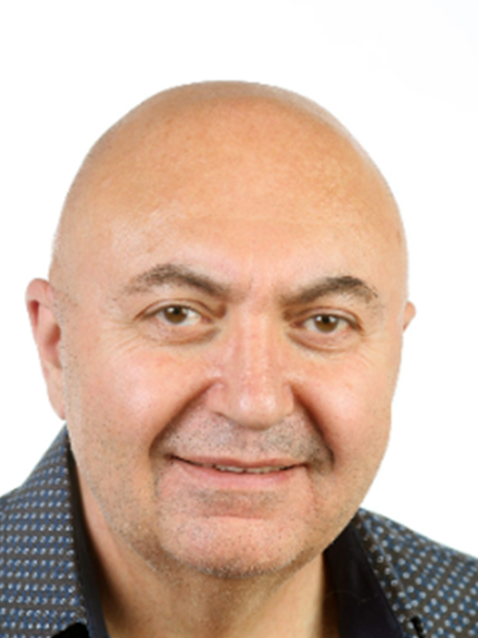
"Accelerating the Future: Silicon Photonics and Advanced Packaging at the Heart of HPC" Sandeep Sane (Lightmatter) |
 |
"Optical Signal Processsing (OSP) for pluggable transcedivers and co-packaged optics (CPO)" Yosef Ben Ezra (Newphotonics) |
 |
"Efficient AI System Scale-Up with Optical Interconnect: Opportunities & Challenges" Sunil Priyadarshi (Arista Networks) |
 |
"Chip-Scale Comb Lasers for Co-Packaged Optics" Frank Smyth (Pilot Photonics Ltd) |
 |
"Co-Design and Co-Process for Co-Packaged Optics - An End-To-End Development Solution" Christopher Striemer (AIM Photonics) |
| ---------------------------------------------------------------------------------------------------- | |
| Adv. Packaging and Emerging Technologies: | |
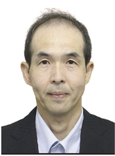 |
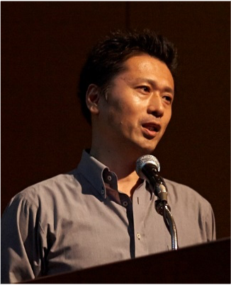
"Thermal management challenges and potential solutions for future flip-chip semiconductors packages" Keiji Matsumoto (IBM Research-Tokyo) |
 |
"Advanced Packaging Technologies for Modular and Powerful Compute" Kazuyuki Irie (GUC Japan) |
| ---------------------------------------------------------------------------------------------------- | |
| Process and Material Technologies: | |
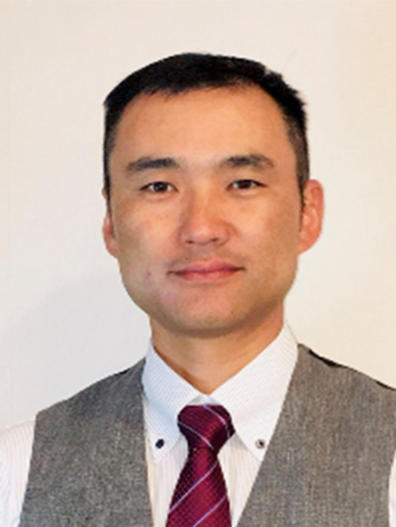 |
""Solution Proposal and Discussion on C2W-HB Toward to Practical Use" ~Introduction of Polymer Dielectric and Mounting Technology~" Takenori Fujiwara (Toray Industries, Inc.) |
 |
"Direct Transfer Bonding Overcoming the Challenges of Integrating delicate and Ultra-Thin Chips with 50-nm Scale Accuracy" Ichiro Sano (TAZMO CO., LTD.) |
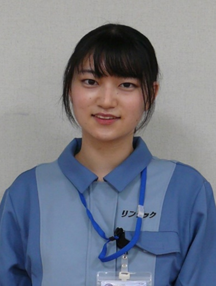 |
"Design and Development of Carrier Tapes for Direct Transfer Bonding Process" Tomoka Kirihata (LINTEC Corporation) |
| ---------------------------------------------------------------------------------------------------- | |
| SI / PI / RF / EMC: | |
 |
"Inductors in Power over Signal (PoC and PoDL) for In-Vehicle Networks" Thomas Schamberger (TDK Electronics AG) |
| ---------------------------------------------------------------------------------------------------- | |
| Bioelectronics and Healthcare: | |
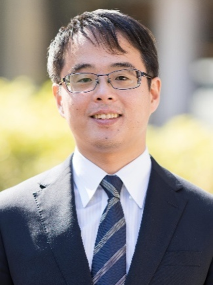 |
"Development of a Rumen Bacteria Microbial Fuel Cell for Cattle Health and Methane Emission Monitoring Devices" Michitaka Yamamoto (The University of Tokyo) |
| ---------------------------------------------------------------------------------------------------- | |
| Power Electronics: | |
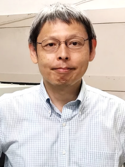 |
"Wafer Bonding of Diamond for Improving Heat Dissipation of Properties of Nitride Devices" Naoteru Shigekawa (Osaka Metropolitan University) |
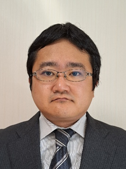 |
"Development of Planar-Gate Vertical GaN MOSFETs" Ryo Tanaka (Fuji Electric Co., Ltd.) |
| ---------------------------------------------------------------------------------------------------- | |
| IEEE EPS Technical session: | |
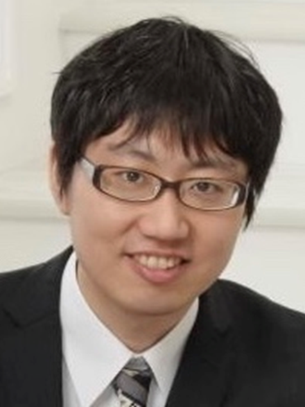 |
"Active optical package substrate with polymer waveguide optical RDL for next generation CPO" Akihiro Noriki (AIST) |
 |
"Fiber-to-chip self-coupling based on near-infrared self-written optical waveguide" Hidetaka Terasawa (Utsunomiya University) |
